The Autumn Smart Watch

Autumn Logo - designed by Jon Ogborne
Greetings, this is a track record of The Autumn Smart Watch Workshop to review our progress throughout the entire process.
The idea of this workshop is to give people the opportunity to play around and customise their own smart watch. The workshop is structured so that it can cater those coming from any background, whether you are an experience programmer, and electronics wizard, or just a person willing to learn, there is something that you can learn during the workshop.
There has been a bloom of smart watch technologies in the recent years and it has been the hot news on every tech news, blogs, magazines, and much more. However, there are still lots of development that can be done in this field. I always like the idea of wearable technologies, having a bit of my own design with me is very satisfying and i want those who share the same thoughts as i do to join the workshop!
The Pictures below are a few of my first designs no custom PCB, all hand made, chunky. However, without these initial designs, it would not have motivated me to be here today. These watches, (and who they are named after) have each motivated and inspired me to do this project. Just a heads up, they don't know about this project as i am writing this post. Its meant to be a surprise.


The Pictures below are a few of my first designs no custom PCB, all hand made, chunky. However, without these initial designs, it would not have motivated me to be here today. These watches, (and who they are named after) have each motivated and inspired me to do this project. Just a heads up, they don't know about this project as i am writing this post. Its meant to be a surprise.

Mark I - Big Daddy, The one that started it all
My Big Daddy, my first attempt at wearable electronics. I don't know about you, but my first idol when it came to designing was from my father. He was a physics teacher and all my fundamental electronics came from him. It was a very crude design and when placed on my wrist, it looks like a bomb! Despite its crudity in look and your negative first impressions, without this first step, the blog would have stopped here and i would not have anything else to say. In terms of battery capacity, non of the watches i have built till this day can beat it, it uses a 2200 mAh capacity! To give you an idea, most of my smart watches as well as all the other smart watches in the market has a battery capacity of less than 500 mAh. This is a beast in comparison!

Mark II - Cherose, after my sister
Mark II, or as i named it , Cherose after my baby sister. Not only because i am damn proud if it, but also because it was completed on her birthday 13th of February. This was my first attempt in fitting all the electronics from the watch above into a small enclosure. From this watch onward, i have used this enclosure on all my watches. ( except the autumn lady which will be mentioned shortly). It uses a 1.3" OLED display, and a 100 mAh battery ( no way i could fit that 2200 mAh one inside!). However, this one does not have an RTC built in, What it does is that when i synced it with the phone, it retrieves the time from it and uses an internal counter to keep count of the time. This was not a success as i would always require to sync it with my phone, and i could not use it whenever my phone was not present. Also, i still could not fit everything into the watch enclosure as you can see from the bulging piece of 4mm acrylic. I knew i could improve it further.

Mark III - Jemimah, after my best friend
Mark III, like Jemimah, when i first saw this watch after completion, i thought it was damn beautiful the same reaction i had when i first saw Jemimah. Some might disagree, but hey, beauty is in the eye of the beholder. The difference between Mark III and II is the implementation of the RTC so that it will work without the need of a phone. Also, however odd this may seem, the time on that quartz clock is not showing the correct time! Mark III is! Another interesting thing i would like to point out is that i have added an extra component inside the watch but have reduced the size of the watch by that extra 4 mm acrylic. This was done by patience and good spacial arrangements. Also, like Jemimah, I think this watch looks sexy.


Mark IV - Eirene, Gaming buddy
Eirene, is a whole new breed of Watches. Like the person i named it after, Its smarter, tougher, and have a love for brown leather. it also has a slightly bigger battery, and has magnetic charging. I have used different internal wiring employing different wire gauges, different slide switches ,a new way to turn off the display when not in use, different microprocessor and best of all, a brand new software.
The new microprocessor , the AtMega32u4, has an inbuilt USB programmer, that means that i don't need an external FTDI connector for the previous 3 watches that uses the AtMega328p. The current microprocessor also boots up faster compared to its predecessors.
The new software makes the watch more memory and battery efficient. The trade off however is this chip has 4 kb less memory. It might not sound like its a lot, but in the hands of a good programmer, it will make a huge difference.
There is also a Tilt switch inside Mark IV. This detects when the watch is on its side or when it is upright. How other smart watch company overcome this problem is that they use an accelerometer, but during that time, i could not physically fit an accelerometer module without creating a customised PCB. Also, having a passive tilt switch means that i don't have to worry about the power consumption on the accelerometer. I might implement one in future designs.


Mark V - Joanne, The perfectionist
The Final one of the prototypes. This was the one i had set as my bench mark! I took the picture sideways because its the first watch i made without any bulge. It was perfectly flat. This watch did not differ much from Mark IV. The only difference is that i used a different wiring method as well as a thinner and a higher gauge of wire making it more flexible. After This Final version, it was the beginning of the autumn generation.
The Workshop Idea
So why A Smart Watch Workshop? We just thought that its a unique idea. There are lots of DIY Smart Watches available on the Instructables website, and this design will probably be very similar to those. For those who do not have the equipment, components, skills or know-how to do as the website instructs, then this workshop will be a good start for you. It is also a good place to meet people who are equally enthusiastic as you are and a good place to realize your ideas. Creating a smartwatch from scratch can be very fiddly, my first design took me 6 hours just to solder all the components together and trying to fit all of it into a small enclosure.Now we believe that a watch is personal, as you saw from the pictures above, i added a different touch to each of the watch. We want you to be able to do the same! In this workshop, we have designed a custom PCB that contains all the useful modules for you to start building the smart watch. Despite having a custom PCB, it doesn't mean that you cannot customize your designs, we want you to make YOUR smart watch.
So how "Smart" is smart? , bear in mind, this is no apple watch or the new pebble time, we are no where near that advance. The watch can be programmed to do what you can imagine it to do and it gives an easier platform to do it compared to the other watches out there in the market. The Autumn smart watch will do basic push notifications from your phone by default and there is room for more! I have tried playing pong on it, snakes, even use it as a remote control to control my lamp! the possibilities are limitless and is only bounded by your imagination, and possibly the micro controllers memory =P. So how smart is it? Well how smart are you?
Week 1 - Designing the PCB
Believe it or not, this is only the second time i have ever properly designed a PCB, so i am open to constructive criticism on how to improve it.
Designed in eagle, the first version of the PCB was a 4 layer board manufactured by OSH Park in america . 2 weeks has past while i write this section so there has been a few modifications to the initial design. The first ever, version 1.0, is made up using a 4 layer board, why? its simple, never trust the Auto router! later revisions, i have manage to get it to be a 2 layer board and also reduce the overall size of the board.

Autumn v.1
Autumn v.1 as the name implies, is the first version of the PCB. As mentioned above, it is a 4 layer board. There are two reasons i went with a 4 layer board actually.
1. I trusted auto router and did not bother to check the number of wires on the internal layers. Apparently i only used a handful of tracks on layer 2 and none on layer 15. but its all in the learning process!
2. So i could have tried harder and fit everything into a 2 layer board, but one of the reasons why i stuck with a 4 layer board was because of the MAX 17043 lipo fuel gauge component. A heads up for those of you making PCB with small clearance for components, OSH parks process of making a 2 layer board gives a minimum clearance of 6 mil, but the 4 layer board gives a clearance of 5 mil. The MAX 17043 package has a clearance of 5 mil between each leg, so that was one of the major reasons for going for a 4 layer board.
For those who are wondering, 3 of these 4 layer boards costs $ 12.

Autumn v.2
Autumn v.2 has a smaller form factor , looks cuter, and it is cheaper. Compared to the first version, version 2 does not use a through hole drilling but uses a SMT pad to save space. It also only uses 2 layers, so the price of the board has reduce significantly. As mentioned above, a 2 layer board has a 6 mil clearance which is not ideal for the MAX 17043 package. But i think it would not matter that much as there should be enough for tor the chip to still work. If after receiving the boards, the clearance is not good enough, i will use a different fuel gauge with a larger clearance.
Unlike its predecessor, this board uses a smaller Bluetooth module to achieve its smaller profile. This board should arrive in 2 weeks from the date of me writing this post.
3 of these boards cost $ 4.40

Autumn v.3 (lady)
Many smartwatches out in the market are predominantly masculine in design and i think that's why we don't see a lot of females wearing smart watches ( or at least i don't). The 3rd revision of the board nicknamed Autumn lady, is designed for low profile, small form factor watch. Most female watches are much smaller than watches male watches, the schematic is almost similar to the previous two, with the trade off of having a smaller battery capacity and a smaller display.
In order to achieve maximum space optimisation, i have removed the USB connector and integrated the 0.49 OLED display. It will be a very tough challenge to fit everything in a small watch case as i only have approximately 8 mm thickness for the PCB + screen + battery. When the PCB arrives and i have assembled the board, I will post and update in this blog. The radius of the PCB is 13 mm.
The price for 3 PCB is $ 5.40.
The experience i had designing the first Autumn PCB was interesting , i used KiCad for my first PCB so i had to relearn how to design with eagle. But with help from my mentally challenged friend Adam Catley, we manage to finish our first PCB and submit it for manufacturing.
Week 2 - Apps
We are not experienced programmers, in particular, writing apps. So during the second week, we researched on how to write apps for both android and iOS. It is still an ongoing process as i am writing this. For the iOS app, i needed to get an apple developer licence from the university, get my device approved, get the profiles i needed and much more. The sad thing is, the universities apple licence does not support the BLE accessories profile, so i could not upload any test apps to my phone. I might have to do more research on how to get the app running. I don't really want to buy an apple developer licence as i am not an avid programmer. However, when i first created my prototype smartwatches, i did not have an iOS app, but i was able to receive notifications from my phone and push it to my watch. This was been made able by apples ANCS (apple notification centre service). It is by far my favourite thing apple has done. If i cannot get my iOS app running, i will be using the ANCS Go and Check it!
The android app will be updated shortly
Week 3 - ordering the components, assembly planning, and receiving the boards(delayed)
After ordering all the components, the first batch of boards Should have arrived by the end of the third week, however due to unforeseen circumstances, The boards will be delayed by a week. i have sent 2 batches of Autumn v.1 to OSH park to be manufactured both on express shipping,
The first batch which was supposed to be delivered on week 3 is currently still held at Tamworth GB and is expected to be delivered on week 4.

The second batch which should be delivered this week had a little hiccup in the production line. The manufacturer deemed that batch faulty and OSH park is working hard to send me the new batch ASAP. This was the email informing me.
Most of the electronic components are ordered from UK mouser . It is not the cheapest option to purchase components from reputable electronics company, I can get components from china for 1/4th of the price, but due to quality control and time constraints, we went for a more reputable company. other sources includes Amazon, and RS components.
From my experience, UK mouser charges 12 Pounds for shipping, where as RS components has free next day delivery. However, a lot of the components i needed was not in stock from RS components. Since UK mouser charges 12 Pounds per shipping for components under 50 pounds, i figured it would be more economical to get the majority of my components from there. The total cost for 6 watches worth of components including VAT was around 70 pounds.
Another interesting fact, non of us working on this project has ever done SMD soldering before! So this will be a very interesting experience. I was given advice to use a laser cut stencil for use of re-flow. I am hoping that during week 4, the universities electrical department can help me with that. Most of the passive components has a 0603 package, and from my understanding, this can be soldered manually. The only problem that we will have is again, the MAX 17043. The package is a TDFN package with almost no leg to be soldered to. This might be easy for an experienced assembler, but for a first timer, this is going to be a new experience.
I was talking to a person at the Bristol Robotics Laboratory (BRL) and he said that he can give a hand if we have trouble assembling and testing the board. Not only do they have the skills, but the tools as well.
Week 4 - Boards and components arriving ,assembly , and testing.

The first batch which was supposed to be delivered on week 3 is currently still held at Tamworth GB and is expected to be delivered on week 4.

The second batch which should be delivered this week had a little hiccup in the production line. The manufacturer deemed that batch faulty and OSH park is working hard to send me the new batch ASAP. This was the email informing me.
Hi Desmond,No point crying over spilled milk, lets hope for the best next week!
I'm really sorry for the trouble on this, but the fab marked all copies of your board from this order as damaged. As a result, we don't have anything to ship you at the moment.
Most of the electronic components are ordered from UK mouser . It is not the cheapest option to purchase components from reputable electronics company, I can get components from china for 1/4th of the price, but due to quality control and time constraints, we went for a more reputable company. other sources includes Amazon, and RS components.
From my experience, UK mouser charges 12 Pounds for shipping, where as RS components has free next day delivery. However, a lot of the components i needed was not in stock from RS components. Since UK mouser charges 12 Pounds per shipping for components under 50 pounds, i figured it would be more economical to get the majority of my components from there. The total cost for 6 watches worth of components including VAT was around 70 pounds.
Another interesting fact, non of us working on this project has ever done SMD soldering before! So this will be a very interesting experience. I was given advice to use a laser cut stencil for use of re-flow. I am hoping that during week 4, the universities electrical department can help me with that. Most of the passive components has a 0603 package, and from my understanding, this can be soldered manually. The only problem that we will have is again, the MAX 17043. The package is a TDFN package with almost no leg to be soldered to. This might be easy for an experienced assembler, but for a first timer, this is going to be a new experience.
I was talking to a person at the Bristol Robotics Laboratory (BRL) and he said that he can give a hand if we have trouble assembling and testing the board. Not only do they have the skills, but the tools as well.
Week 4 - Boards and components arriving ,assembly , and testing.

Yay, the boards arrived from OSH park in glorious purple! And my first inspection of the boards did not disappoint us. As planned, the rest of the components arrived and we went on to the electrical labs to assemble them.


Board held down for soldering
We carefully held the board down using the most advance techniques to ensure minimal movements during our work. As you can see in the photo, we have a schematic print out of the board so we can place components without hesitations.

Haziq trying to solder
The tedious process begins. we spent a few good hours assembling the first board despite it being small. This was our first time doing a full SMD board and we were a little nervous, but after a few practices, it became second nature.

Our First Autumn Board in all its purple glory
Done! our first board was finished ! we could not wait to test it! This was our first assembled board, and we were quite happy with our work

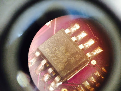
DS3231MZ+ under inspection
Of course, we could not just assemble the board without inspection could we, we had to ensure that all the joints had properly been soldered down and it had a smooth and shinny solder coating on it.
Testing the boards
So, it was this stage when we bumped into an error, We could not run the boot loader on to the board as we forgot to include an SPI output for the AtMega chip to be programmed! but by careful soldering, we managed to somehow cheat our way through.
Now, the initial PCB layout that we designed was not optimal, i will list the problems that we had with it.
1. We read up that the AtMega could run of its 8Mhz internal oscillator and it could still work with its built in USB functionality, however, it would be slow and unreliable. After careful reconsideration, we decided that we should include it as this PCB will be used for a workshop and we should keep in mind that there will be participants with zero knowledge on how to face these types of problems. So we Modified our schematic and created a breadboard layout to ensured that it worked
2. We decided to remove to battery monitor. This is because we did not need a 0.1 scale division for the capacity, we actually only need 3-4 indications ie. Fully charge, half charge and recharge. And we plan to achieve this by monitoring voltage. Normally, it is not ideal to monitor voltage alone as it does not give an accurate indication due to the characteristics of a battery discharge curve, but so long as we keep it within range, say above 3.3 V, and any lower we throw a recharge distress and the watch will go into sleep mode when it drops bellow 3.2V. This is to ensure that the battery does over discharge to prolong the batteries life span.
3. The lipo protection circuit is designed to ensure that the battery does not over charge. Initially, the idea was to put the circuit outside to save space inside the PCB. But after much consideration, we decided that it would be safer to include it in our internal design so that users do not need a special cable to charge it but can do so with a normal micro USB cable. After all, the safety of our participants is our top priority!
We did not waste any time and started work immediately, we followed our new schematic and created a bread board layout

The bread board layout working
So even the breadboard layout had some issues. For example, the pull-up resistor for the I2C lines are typically in the Thousands of ohms, mine only works with 132 ohms on the SCL line. Any other values will break it. I suspect that there might already be an internal pull-up resistor somewhere but continuos testings will be carried out. Whats EVEN stranger is that the I2C only works when it is plugged in to my Mac!! So the board has 2 I2C devices, the Screen and the RTC. i Wrote a simple code to display the time on the serial monitor of the arduino IDE which i have done thousands of time. I have two computers, a mac and a windows, and for some reason, it only works on my mac and not my windows. Without any pull-up resistors, i can read the time without fail on my mac, but not on my windows. i needed to add a very specific value of 132 ohms on the SCL line for it to work on both machines. There was another weird phenomena, it only works on one of my Macs USB ports........IF i plugged it into the second USB port, it only works for a while. Now, i dont know whats going on, something spooky perhaps, but i got it to work for now. It is either my setup or i have damaged the I2C part of the AtMega, but i will continue testing for the time being.
Week 5 - Workshop preparations and More Testings
We Started planning for the workshop about what we are going to do and how we are going to do it. On Monday, we all sat down discussing what we thought the workshop should be. So during the weekend of week 4, myself and Haziq prepared some materials for the proposal meeting. We were trying to come up with a Fun , interactive workshop that everyone of all ages would enjoy.
The pictures bellow Shows our first draft of how we would try to explain the concept of classes in the form of hardware and electronics. We will be using electronics 101 which is parallel and series circuits to explain which blocks or classes are important. For example, one of the blocks called Screen is under a vital block. If we remove this block, the circuit breaks as it is in series ti everything else, and it should, because if you change the class for example modify the screen driver, the hardware will stop working.
The Parallel block are the non vital ones such as the notification block. If we remove this block, the circuit will still work, but it wont carry out the specific functionality. In our case, If we remove the notification functionality, it will still work as a watch, just not a smart one. So in our board, if you remove a vital block, all the LEDS will die, however if you remove the non vital blocks, the "Smart" LED of the Smart Watch will turn off and only the "Watch" will be illuminated. This is only draft 1 and the idea will be continued to be refined until we feel that it is a good representation of the concept.

Schematic of the board
As electrical engineers, our minds are inclined to think from this perspective. I think its very interesting to be able to explain programming theory in a tangible way. I find it easier for myself to learn from experimentation rather than just theory alone. A better way of saying it would be i remember things better once i actually play with it.

The Block diagram
The crudity of a pen and paper sketch has an odd charm to it. We could have used paint to do this, but hey, archimedes drew on sand. Sure the computer was not yet invented, but i am sure they had paper back then which was probably equivalent to our computers these days. Anyway, enough of me trying to justify my laziness.
Hardware and Software Testing stage 2

Power Management Testings
I am very proud of this design as it should save a ton of power, and thats what we want in a smart watch. My previous designs could only last 8 hours because i did not have a smart way to put the micro controller to sleep. From my experience, The Sleep library on the arduino is fiddly, and is fairly annoying to implement both code and hardware. Being an electrical engineer, I wanted a more electronic approach to solve power issue.
I used a soft latching IC (Insert model number), an op amp and a transistor to solve this issue. The button turns the IC on and Off, the output of the IC is used to turn on transistor which drives the micro. So how can this be used to save power? So after a while, the micro can trigger an event which turns itself off(suicide). This is like a timeout on most sleep/wake button on your phone, but instead of putting it to sleep, it turns the micro off. What happens when a notification comes in while the micro is off?
I used the RX signal of the Bluetooth module to trigger the IC to turn the Micro on. However, the amplitude of the signal (voltage) was too low to trigger anything. So i used an OP Amp to amplify the signal to trigger a turn on. Some of you might be wondering now that since i am using the RX signal to turn it on, doesn't that mean i am loosing data? yes we do loose data, but we can always request for more! Ask and it will be given to you (Mathew 7:7).
So, in a nutshell. The only thing that is constantly on, is the BLE ( bluetooth LOW energy), The RTC (runs for years on a battery) and an OP-amp which might draw some current(0.4mA)
edit: So To the previous statement, The BLE is not so Low energy after all. At normal modes, it draws about 8mA, not much but for a standby current but it would only last about 24 hours. 8mA is what the data sheet says it would draw. I have not been able to put it in sleep mode as of yet which draws 10uA. When i say, not able, as in a know the protocol, i know the commands, but it is not ideal for my situation. In order to wake the BLE from sleep mode, the user is required to send a random string to the BLE of length > 80 and it does not expect any AT commands. As of writing this blog, i have realised that the Sleep function does not work while in ANCS mode. I probably have to disable ANCS mode before entering sleep mode. Further testing shall continue!
Working frequency:2.4GHz ISM band .Modulation method: GFSK(Gaussian Frequency Shift Keying) .RF Power:≤4dBm, Class 2 .Sensitivity:≤-84dBm at 0.1% BER .Speed: 2.1Mbps(Max) / 160 kbps (Asynchronous), 1Mbps/1Mbps(Max) (Synchronous).Security: Authentication and encryption .Service:Working temperature:–5 ~ +65 CentigradeFlash:256KbPower: 0.5 mA for standby, Active 8.5 mA,supports auto sleep.
This is the value i was Getting. Now all i need to do i reach that 0.5mA.
edit: An hour after writing the above statement i did some more testing and i think i might have come up with a solution. I am using a Vici multimeter , A Fluke ripoff (more or less). I would use better multimeter if i had one, but this one does a decent job as you can see.

Active current of BLE
As explained earlier, the current draw is 8.5 mA which is as described in the data sheet.

Standby Current of BLE
So I have found an interesting setup using the AT commands to save power. Basically, When the BLE is not connected to the iPhone, it will automatically go to sleep mode and draw 0.5mA. When i turn on bluetooth on my phone, it jumps back to 8.5mA. For the time being, this is the best setup that i can think off without complex methods to solve the situation. But maybe, we can utilise this to our advantage. Now, we have an easy way to save power, not necessarily the best way. The user can swipe up to their control centre and just tap the bluetooth icon, and BAM, the current drops by at least 10 folds. Also, Once the watch is idle mode, switching the bluetooth on turns the watch on. This is of cause all reprogrammable. A more advance user could probably find a better method to save power, but as of this moment, it is not within my capabilities.
Another interesting thing about this setup, is that when the watch looses the bluetooth signal of the phone, it automatically puts the BLE to sleep. So it could even be a feature. I have to admit that i have a dream to make this a decent watch but i doubt i will be able to come close to the pebble smart watch standards, but i will try =)

The current draw for the whole test board
This is the total current roughly being drawn from the power supply which was what i was expecting. The Oled screen sucks power like a sponge! but its cheap and it looks sexy.

Idle Current Draw
This is the total current being drawn at that moment. I think this is a great achievement for me being able to reach the uA range =).
Just a side note, being able to achieve about 10mA idle current is actually a vast improvement for me. My older designs had a constant current draw of 50mA give or take. So even if i cant achieve my desired uA current consumption, it is already a great improvement.

Newest team member - Josh
Commencing into our second month of the project, A new member has been added to our platoon! Josh has a Masters in Computer Science and he will be helping us with the structuring of the code. Previously, i have written the code for the watch, but it was a "spaghetti" code as Richard Grafton called it. It did not have classes, no headers, and the whole flow of my code was confusing. So for the sake of the workshop, Josh to the rescue! With his help, the participants of the Workshop wont have to worry too much about the code, or if they want to modify it, there will be classes written to assist them.
Week 6 - Circuit finalisation
The end is coming near as Week 6 approaches. However, we are still going strong and there has been good progress on the project. Firstly an update on the Circuit
I have done some more testings and experimentations on the circuitry and trying my very best to optimise power consumption on the circuit. For the bluetooth module and the AtMega to Work to its maximum performance, the circuit has to be powered by 3.3 V. And initially i did not know this, the data sheet of the AtMega32u4 states that it goes up to 5.5 V but experiments says otherwise. I have tested the Circuit at various voltages using various converters and the conclusion that i came up with was to use a 3.3 V linear regulator to drive the whole circuit. The thought of using a buck converter did cross my mind and i actually have experimented using buck converters but i will break down the reason why i have chosen this option.
So a few things to know. Generally, Linear Regulators are inefficient as they remove excess voltage in terms of heat. while a buck converter uses PWM to control the output voltage so it can get an efficiency of about 90 % or more. However, they are normally complex in design and more expensive. And after doing some experimentations i will elaborate why a linear regulator is more suitable as of this moment.

Measured using my Hitachi analog oscilloscope
The image above shows not the DC component of the power supply but the AC ripple coming out of the Buck converter. Using my multimeter it reads a nice 3.333 V output but my circuit would fail and i could not explain why. When i powered the circuit using either a 3.3 V regulator or from direct power supply, it worked like a charm. It took me a few days to figure out the amount of noise i had on the Buck converter output. So a useful thing to note is that i have set my scope to 50 mV per division. That means that i was having a 200 mV peak to peak noise which would have caused my buck converter to go out of spec. A way to remove the noise is to use decoupling capacitors on the power rails, and it did lower the noise significantly, but it was very unstable and would still fail after a certain period of time. Despite being more efficient, it adds a larger hole to our pockets as well compared to a traditional voltage regulator.
Using voltage regulator, i was barely getting any noise on the AC mode of my oscilloscope which is good. I believe that poor setup of the buck converter caused such noise to occur. The problem i worried about the linear regulator was the horror stories of it being extremely inefficient and it is true. If a am dropping 12 V to 3.3 V across a load that draws say 100 mA, thats 870 mW of power being dissipated which gets really really hot. and at that point, the regulator is being extremely inefficient at only approximately 30 % efficiency. However, a good property of the linear voltage regulator is that once the input voltage approaches the value of the output voltage as a typical battery discharge curve will show, the efficiency actually increases. Plus, i am only dropping 4.2 - 3.7 V to 3.3 V which is
0.9 V drop at most and drawing 40 mA at worst case. At sleep mode, the circuit should only draw about 0.8mA which should not matter too much.
The verdict?
There is obviously pros and cons to any design choice and this is one of my first real choice when it comes to designing a board that other people will be using. And as of this moment, i believe that the 3.3 V linear regulator will serve the job better. Not only it being cheaper, smaller , simpler as well as having less noise, coupled with the fact that i am not dropping much voltage, it could be the more sensible solution. However, i could be wrong and i am open to any suggestions to help me improve this design.
The battery charging circuit
It is very important that the lipo battery does not over charge or over discharge as it will shorten the life of the battery dramatically. My initial idea was to put the charging circuit outside of the watch as it wont physically occupy much space, but i think the safest way to do it is to incorporate a charging circuit to ensure maximum safety irregardless of what charging cable they might be using. If the watch did not have a protection circuit, the user had to use a special cable to charge and program the watch as the cable would include the charging circuit, but hey, if i was a user, i want to be able to use any cable i want and not have to remember to bring that specific cable.
So this section explains the charging circuit test bench.

3 multimeters to monitor the circuit
In this picture, i have 3 multimeters to monitor the lipo battery charging process, but actually i had another Am-meter monitoring the current draw of the circuit.
So, my cheap multimeter ( i am sure you can guess which one) is monitoring the input voltage. My Vichy ripoff multimeter(yellow one) is monitoring the logic level of the circuit. I will elaborate later. and my new Uni-T 61E which arrived today(You can see the manual on the left) is monitoring the charging voltage. A good voltage to charge is at 5.0V as that is what the USB carries in terms of voltage, but for that instance, i took it at 4.5V just for safety. This was charging a 4000 mAh ultra fire 3.7 li-ion battery which took almost forever. My Vici multimeter monitored the logic state which is logic 0 for charging and logic 1 for fully charge and it is supposed to be connected to a micro controller to detect the logic state and determine the state of the battery to inform to the user. As you can see, a fully charged li-ion is meant to be roughly 4.2V so the logic level is still at logic 0, bellow 2.5 V. The Uni-T is reading 4.06V which seems fairly close to 4.2V, but bear in mind that it is a 4000 mAh battery, so it takes a while!.

100 mAh Lipo being charged
Now, i could not wait that long, so i hooked up a more realistic example using a 100 mAh lipo charging at 5.0V. Everything went smoothly surprisingly, the charging voltage went up steadily, the logic level reached 4.5V as expected, and the current draw went to 0 A at the end of the experiment. So all the theoretical parts were fulfilled! Wohoo! So once this section is done, all that is left is the button....which should be fairly simple, but i thought the power supply would be simple, so i might be in for a surprise.
Things i have found out over the pass few weeks
So a lesson that i have learn so far is that check everything and that most errors are often the simplest of all. When the I2C line was not working on my circuit, i thought to myself, "Oh it must be the Signal of the lines, or it could be the internal pull up resistor. Or maybe it could be the parasitic capacitance of the breadboard,Voltage incompatibility, current limitations, noise, faulty components or maybe even poltergeist!!!" Although it could have been all of the previously mentioned, yes, even poltergeist, it wasn't it was human error!

BAD SOLDERING!
As you can see, it was just very very poor soldering! You cant see this, but this section of the AtMega is pin 18 and 19 and for those of you who don't know, those are the I2C lines!!!! We tend to over think situations, but always go back to the basics before jumping to conclusions! Also another good tip is to use good soldering tools which includes a variable temperature soldering iron, Flux, inspection tools and a good soldering tip. contrary to popular believe, a fine soldering tip is not necessarily the best for SMD soldering. A chisel tip is actually much more efficient as the heat is focused on the tip unlike the sharp pointed tips where the heat is mainly focused on the side of the cone. A good solder tip should be able to heat the legs as well as the pads simultaneously at the right temperature. Variable temperature is important as a high temperature might destroy the traces on your PCB! Trust me, i have destroyed a few traces before because i did not know this!

Better soldering
The circuit started working after i improved the soldering. This was not the only one, there was also the RTC which was poorly soldered on! so a lesson to be learned, use a microscope to check everything! if you don't have a microscope, use a 30X magnifier like i did in these two photos. i just used a jewelries inspection microscope and hooked it up to my phones camera. quality is surprisingly
good =)
Software and hardware
This week, we are planning to merge software and hardware together to test if everything is working. Hopefully we can come to a conclusion fairly quickly as i have to consider manufacturing time as well.
Full hardware test

Workshop video
Software and hardware
This week, we are planning to merge software and hardware together to test if everything is working. Hopefully we can come to a conclusion fairly quickly as i have to consider manufacturing time as well.
Full hardware test

Full breadboard setup
So, this is the full board setup! a quick breakdown, the blue breadboard is the power manager. It controls the on and off of the entire circuit. The white breadboard on the right is the AtMega 32u4 breakout. The smallest one controls the charging circuit. Everything works fine on breadboard! so the next thing to do is to set the schematic up!
Workshop video
Battery charging video
Every Workshop would need to have a interactive way to demonstrate what we are trying to explain in a simple and fun way. And i believe we should be able to explain basic electronics to everyone using a method that they can relate to. The Battery charging video is made to show participants about the basis of the battery discharge curve. Now, we could just show the battery discharge graph and explain to the participants based in that, but that would seem to theocratical and rather boring. So this particular video is only 60 seconds long as we try to keep it short and simple.
current consumption video
We believe its important to explain the concept of current consumption to our participants especially for the young. You will notice that the videos are design to not explain the concept like how the university would. People who do not know about electronics wont want to hear about ohms law straight off the bat, its too technical! both my mom and my best friend Jemimah are teachers, my mom has been teaching for more than 25 years and Jemimah is a teacher in training. Both of them gave me the same advice, which is to use examples which can be found on a daily basis to get kids in particular to be interested in the concept. one they are hooked, they reel them in with some theory.
However, we also know that not everyone is the same. Some people want more theory and others want more hands on experience. We all learn differently. So we have to ensure our workshop caters for both kind of people. We are still structuring our workshop and we know that at this point, the best way to know for sure is to do a field test. At the end of august, we will have participants of all ages and see how effective is our technique.
Workshop manual

Week 7- PCB design round 2


Week 7 was my second attempt at the PCB design stage. some might say it is a waste of time making the PCB twice. But i believe it gave me the ability to produce a better PCB the second time. After receiving the first batch of PCB's i realised that there was so many things that can be improved. the keep out warnings in eagle are unnecessary. Autumn 1.0 had the resistor spacing too far apart, it used through hole components which was silly of me, the DRC was not optimised, i did not take into account the actual layout of the case itself and many many more things that i could improve. Other than the layout, this also features an upgrade as mentioned in the previous section on this blog.
I believe i made a major improvement in doing the schematic layout as well. initially i used all connecting wires which made the whole schematic unreadable and messy. There was no proper flow in the schematic diagram. Autumn 2.0, i used labels to represent the wires. it made the schematic so much easier to read and understand. I also put a little bit more effort as to where i placed the components on the schematic layout to give myself and whomever reading in the future a better understanding of the flow.
The PCB layout has changed significantly as well. I incorporated an L-layout so i can add the slide switch on there. previously, i would super glue or i would have used super glue to stick the switch on the side plates, which was not the best idea. So this time, i took that into consideration and added a side panel that the switch can fit on. I also took into account the size of the battery and where it will physically fit on the board. the L cut out is the exact cut out for the battery to fit in. The buttons are also now mounted straight to the PCB so i dont have to fiddle with the side panels anymore and make the watch build abit more consistent. Overall, i believe that this layout is an improvement to the last.
This time i went for Ragworm which is a UK based company. I also opt for express shipping so i could get the boards a few days earlier. Hey, time is very crucial and the sooner i get the boards the better. In retrospect, it was a good decision.
Week 8 - Finishing touches
Workshop manual

The Autumn Workshop Manual
Because all of us needs a book telling us what to do. This is just the front cover of the manual of cause. There is still lots to be written in this book. Haziq is currently taking care of this.

Autumn 2.0 L- layout

Autumn 2.0 Schematic diagram
Week 7 was my second attempt at the PCB design stage. some might say it is a waste of time making the PCB twice. But i believe it gave me the ability to produce a better PCB the second time. After receiving the first batch of PCB's i realised that there was so many things that can be improved. the keep out warnings in eagle are unnecessary. Autumn 1.0 had the resistor spacing too far apart, it used through hole components which was silly of me, the DRC was not optimised, i did not take into account the actual layout of the case itself and many many more things that i could improve. Other than the layout, this also features an upgrade as mentioned in the previous section on this blog.
I believe i made a major improvement in doing the schematic layout as well. initially i used all connecting wires which made the whole schematic unreadable and messy. There was no proper flow in the schematic diagram. Autumn 2.0, i used labels to represent the wires. it made the schematic so much easier to read and understand. I also put a little bit more effort as to where i placed the components on the schematic layout to give myself and whomever reading in the future a better understanding of the flow.
The PCB layout has changed significantly as well. I incorporated an L-layout so i can add the slide switch on there. previously, i would super glue or i would have used super glue to stick the switch on the side plates, which was not the best idea. So this time, i took that into consideration and added a side panel that the switch can fit on. I also took into account the size of the battery and where it will physically fit on the board. the L cut out is the exact cut out for the battery to fit in. The buttons are also now mounted straight to the PCB so i dont have to fiddle with the side panels anymore and make the watch build abit more consistent. Overall, i believe that this layout is an improvement to the last.
This time i went for Ragworm which is a UK based company. I also opt for express shipping so i could get the boards a few days earlier. Hey, time is very crucial and the sooner i get the boards the better. In retrospect, it was a good decision.
Week 8 - Finishing touches

Me and Connor from Ragworm
Well well, what do you know. I actually got the chance to meet the guy that actually help make my PCB from last week! He was there at the bristols Mini makers fair and he happen to remember my name from my PCB submission last week. That was the highlight of that day.

Autumn Boards
It came in an airtight bubble wrap!! very beautifully packed. As you can see, i made 3 different variations of the same schematic with slight changes in each one to suit the designs specification. I will now reveal some of the derivative of the main design =)

The PCBs ready for assembly
On this table is a list of my PCB practices. practice makes perfect and at the end of this section i will show you the differences it made for me. I am still very new in PCB designing and this is my autumn v2 is the results of my past failure. Don't be afraid to fail. Learn from it and it will make you better.
At the same time , some new components arrived.

My kitchen table no longer a kitchen table
I ordered 90% of my components from RS components this time, some left overs from my first batch, some from Farnell and a slide switch from amazon. There is something very interesting that i would like to point out. On the kitchen table lies a very international group of item. I have components made from China, Japan, Israel, Mexico,Thailand,Taiwan,Hong Kong, United Kingdom, America, and MALAYSIA! Yes i am Malaysian. I had a lot of issues with delayed components. RS claims next day delivery, but until today, they still have not delivered my 2K 0603 resistor!!!!! every time i email them, sent them a chat on their website, they will say " it will be with you tomorrow" but its been 2 weeks now =(, very disappointed. Farnell on the other hand has been very on schedule, Big thumbs up!
Now, From my previous experience assembling the first batches of boards, I did not incorporate and SPI pins and i did not know i could not boot load from the USB. Sounds silly now, but in retrospect, i did not know. previously, this was how i boot loaded

Board being boot loaded
I wont go through how to boot load the AtMega here, you can find clear instructions on the main arduino website. This was a poor, sloppy method to burn the boot loader, and i was very unhappy with myself for this. Even though now, autumn v2 has SPI pins to boot load, i did not want to solder wires to it to boot load, there has to be an easier way. So, i made this!! ( it was sooooo worth it)

My own bootloader
Tadaaa! isnt she beautiful! i botched it together myself =) and when i say botched, i really mean it

Botched job
This was how i did it, i did not have the time to make a custom PCB for this, so i went all old school and made a Vero board botched job =) it essentially is an arduino. with its own oscillator, decoupling capacitor and all that good stuff. The only difference is that it has a TQFP- 44 socket that i can easily remove the burnt chip. It took me a whole day of intense concentration to do this. To my surprise, it actually worked first time around =) so i was very happy with that. It also has the 3 LED indicator to know the heartbeat of the Chip. Those of you who have used arduino as an ISP will know what i am talking about.

AtMega being Boot loaded
This is more handy than you think, i am assembling many many boards for the use of a worksop. It just makes life easier, but hey, to each their own =) im just too lazy to manually solder and program so i made this! i call it charcoal because it burns the AtMega =P . And i just could not resist making a 3d printed case for it, i just could not help it =(.
Anyways, after burning the firmware, it now can be officially used on an arduino IDE! Now this is where the fun starts! The assembly line! Previously, We assembled the first board in the university lab because i thought it had all the tools required to do the job. But i could not work till late hours and i could only solder there when there was a lab assistant there. So i wanted to solder at home. Now i have been soldering for years, but i have not touch SMD soldering. So i thought that you require advance tools for the job. Proper microscope and all the techie stuff. Turns out, all that i really needed was a pair of steady hands, decent equipment and patience. All the Autumn V2 boards were assembled by myself in my room using only my tools and no lab equipment. Please don't think that i am bragging, my equipment is probably the same as yours, A Maplin Soldering station, A Hot air rework station, a cheap 20 dollar PSU, flux, and solder. The point i am trying to make is that be confidant with yourself. You do not need top quality things for SMD soldering. Haziq has written a blog post on it, go check it out!
Yes, it is best practice to use ESD Matting which is heat and chemical resistant, or a anti static brush, and maybe even a high quality tweezers! If i had the cash i will get it, but hey, i'm just a student, and i cant afford these equipments. I did not want to damage my table, so in alot of my pictures, you will see a Paper cutting mat, and occasionally a ply wood for when i am using my hot air gun. I used a tooth brush for removing flux, and a pair of tweezers i got from Wilko in the beauty department. An engineer has to be resourceful.

First Completed Autumn v2 board
I am very happy with the out come of the board! I took a lot of precaution in soldering this board inspecting every joint multiple times. However, problem are bound to occur, and for me, the USB worked fine, i could upload codes to it. But the transistor was heating up to about 100 degrees C! I was worried and checked everything again and again, but i still could not find the problem.
I checked the schematic again and again making sure that i followed exactly on how i wired my breadboard and everything was fine. I finally solved the issue, and can you guess the issue? it was bloody poor soldering again!! well, it was not exactly poor soldering. It was me being careless. But trust me, 90% of the people reading this right now would not be able to spot it.

Spot the short
So, who can spot the solder short here? remember i mentioned that i inspected everything under my magnifying glass ( too poor for a microscope ). Still cant see it? let me zoom in some more! Note, this was taken using my phone through the magnifying glass.

Capacitor - vias Short
So, this was the issue causing the transistor to heat up. whenever a problem occurs, i always doubt my schematic and my design and i always over complicate the issue. So a tip for anyone out there, check your soldering under a microscope if you can. I actually spotted this mistake by chance. I was playing around with my Uni-T multimeter on continuity and i had a beep on VCC and GND! Now you might be wondering why could i upload codes if there was a short? its because there are two isolated Ground in this system. and the GND that was shorted was the one connected to the transistor and not the AtMega. So after a quick swipe with my soldering iron....

First working PCB
BREAKTHROUGH! That was what i told my university supervisor when it worked! You have to imagine my feeling right now =) I was very nervous that the PCBs might not work, and it wasn't initially. I thought that i would have to remove the transistor for good if i screwed up my schematic design. But once i cleared that bridge, BAM! screen turns on and everything worked =) Even the bluetooth!!
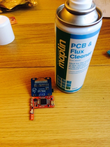
Clean up
Another Maplin product! this time its the PCB & Flux Cleaner! Warning contains isopropanol that feels like ice when it touches your skin. Seriously, i sprayed it outside my window, and i swore i saw ice forming. So Normally after a soldering job, there will be a lot of flux residue. It makes the board all sticky and yellowy and it looks ugly. So we can clean it with Isopropanol. As mentioned above, i used a toothbrush to brush off the dissolved flux off the board.

Board fitting
The battery fits in nicely in the case. I took a lot of aspect in designing this board to make it as neat and professional as possible. i learned my mistake from my previous board. Previously having limited experience with PCB making, i did not take into account the battery location and the entire repeatability of the board. I use the word repeatability because the previous board can still be used, but the location of the slide switch and the push button wont be on a single board and it is very hard to replicate it exactly. So when designing the case, i might run into more problems. I thought that it will be better if i incorporated everything onto the board.

Autumn Backplate
The funnest part! Designing the outlooks of it! Here, i used a 0.8 mm ply wood and a laser cutter to cut and engrave the logo. Initially i wanted to use a milling machine, but the university would not allow me to use it. In my workshop, participants will be given choices, to either use it as it is, or customise it to their hearts content. I made a few variations myself, Carbon fibre, leather as well as my own hand drawing of a pretty sunset i remembered from my home town.


A choice of carbon fibre, plain, with the autumn logo, or choose to leave your own mark. Who does not like a customisable watch?
In the midst of all this excitement, i want to reveal another watch design =) There is nothing wrong with the Autumn watch, I will want to wear it =) but i know that a chunky design will not suit every wrist, so that is why i designed this new breed of watches. I call it the Autumn Colours

Autumn Colours

Autumn Colours V1

Autumn Colours V1- Cathy
Why? Well the story goes way back when i was designing Mark II of Autumn. I went to Sainsbury one day and i saw this glorious item on offer.

Fitbug Orb
Note that the normal price is 20 pounds, but i got it for 6.99 that day =) So here is the story and why this watch means so much to me. It would be amazing to be able to design my own case, i would really love the opportunity to do so, but it requires lots of money and i don't have that kind of money. I have to rely on off the shelf products and build my design around it. Also it shows resourcefulness, i mean i got it from Sainsbury! Of all places! This item was sitting on the shelf for months and nobody bought it, i bought my second box a few days ago because the first batch was for testing.
So while i was walking down the reduce section, i saw this wonderful item on sale. Of course, my mind was already thinking about the watches, so the thought that came to my mind was "Can i use this instead?" it looks cute, and to get everything to fit would be wonderful! Now if you look back when i was building Mark II, i had problem fitting everything into that big case! how would i be able to fit an arduino into that thing! Back then, i had no PCB building knowledge yet, i had to rely on off the shelf modules like the arduino pro micro and the RTC modules. It was only last week (24th August 2015) when i manage to fit everything inside.
My housemate said to me that he was very surprise i could shrink Mark I into the size of Mark II. But trying to fit it into this rubber strap is a whole new level! He said that it cant be done! Well Look at this! it Fits beautifully! He drove me to achieve this, i accepted his scepticism as motivation for me to keep pushing myself to be better. It was the same as battery life. He was the same person that teased my watch to only have 8 hours of battery life. Thats why in Autumn design, i paid so much attention into trying to conserve battery power. An advice to all whom is reading, theres no better feeling than to prove someone wring, and although you cant achieve it back then , that does not mean you wont be able to do so in the future.

Autumn colours
Autumn colours is built upon the same schematic, so the code works the same for both watches. Hopefully with this design, More girls will be interested in electronics =) Also, i am sure my sisters would prefer something like this compared to the beefy Autumn. Why this Shape? there Is a very good reasoning behind it. Like the autumn watch, i use a 0.96 OLED screen. As you can see, i added a through hole component unlike the autumn which uses an SMD pad. This is because autumn colours uses a rubber strap which the users can change the strap easily. I did not want the screen to be connected via wires as it will reduce its rigidity and potentially break. The shaved sides is to give the watch a roundish look.

Autumn Colours
This is how it looks like after fitting the PCB into its rubber case. It actually worked first time around without me having to check all the solder joints again. I designed the board so that the top part is not as bumpy. This will allow the screen to lie closer to the board and this saving space! because at this point, every mm is precious!

Autumn Colours Working
I added a USB port for ease of programming. Unfortunately, i did not want to charge the battery from the USB due to mechanical stress. I did not want to damage the USB as it is a pain to replace if anything goes wrong. So i created a separate charging pin. Its the same for the autumn board as well.

Cathy modelling for Autumn Colours
Final Touches
So what now? As the project quickly approaches its final days, this is what is left to do and we really need to push for it.
1. PCB - I am proud to say my PCB is done and is now currently in the hand assembly process. I don't really want to rush this, as it is manually assembled and rushing this process will result in sloppy job. I still cannot put it all together because that 2K resistor is still not here! I checked today and it will be delivered on the 2nd of September -.-. I will see if i can make do with other values.
99% completed
2. Case - The cases have all arrived and is waiting for assembly. I have laser cut all the pieces and is also ready for glueing. I also have all the materials required to decorate the watch such as the carbon fibre, leather and plain decal. The screen will be made from either tempered glass or PTFE, both of which i have. Its just a matter of which one looks best.
100% completed
3. Charging cable - Unfortunately, the user cannot charge from the USB. Why? its because i wanted the reduce mechanical stress from plugging in the USB. Also, of the user is happy with their software and wants to close up the opening for the USB, they can as i have a small charging port they can use. I have a working prototype, but it is currently 3D printed and it looks ugly =(. I have to think of a more suitable alternative for the long run but it is not a major issue as of this moment.
100% completed
4. Software - The software is still currently in development . Josh is still structuring the code to make it as neat and as user friendly as possible. The code works fine, but its structure is all spaghetti like. Josh says he can finish next week and hopefully everything will work fine. Since there were 4 sections for him to do, and he has done 3/4 of them. I am also required to understand the code like the back of my hand as i will be tested on my code that has been restructured. Shouldn't be too hard . So i would say we are
75% Completed
5.Workshop - The Workshop is still shaky. That is because we do not have a finished code yet and it is very hard to imagine what to do. We are thinking of a trial run with some university students and get some feedback from the workshop to see which aspects are most important. We should be doing the workshop next week. Sad to say, this is probably our lowest completed percentage. However, it takes only one try to get a good structure. All we need to do is finish the code, assemble the watch and try it out. It is the last step of the project and it needs to be executed well.
50% completed
Overall score after 8 weeks?
85% completed
Week 9 - Can we reach 100% ?
Finally the 2K resistors arrived! This means i can test the charging circuit and make sure this watch is actually safe. I mean i have tested in on the breadboard, but not on the actual PCB itself

Charging the watch
After hooking up the rails to 5v, the device was drawing about 500mA initially and slowly dropped to zero which is what was expected. The batteries were brand new so to charge the battery to a 100% takes about 2 hours. I was there for the entire 2 hours worried that something will go wrong but thankfully, everything went well. Furthermore, the full charge indicator works perfectly. When the battery is fully charged, the charging circuit informs the arduino by giving a HIGH on one of it output pin.

The first battery powered Autumn
There is only one thing left to do now for the hardware.....
Assemble!
Because the case is conductive, i needed to protect the circuitry incase of any accidental short. I used electrical tape for this process. its cheap and it gets the job done.

Electrical tape everything
After Insulating everything, here comes the funnest part, the actual fitting into the case!

Assembled Watch
As you may have noticed, i actually sawed off a small part of the case. This is to achieve better fitting of the circuitry.

Manual Labour
No, there was no advance tools for this process, this process requires a bit of skill. You can apply too much pressure from the vice, or else the case bends, but not too little or else the case moves. When you cut the case, you have to be careful not to scratch the front. I have had practice from the first batch of watches, so doing this again was not too hard for me. Here is a time lapse of me assembling the watch. It comes in two parts, the first is me assembling the screen and the vibration motor. I stopped because i needed to charge the watch battery. The second video is of me assembling the actual case.
Part 1 Assembly
Part 2 Assembly
I only have 2 available screens at the moment as the rest are still on delivery. But these watches are working perfectly! Well, thats not true. In my excitement to assemble the watches, i actually forgot to solder the vibration motor on the the black watch....oh well.

First two watches

Fits my wrist perfectly
Well, this has been fun! Unfortunately I still have 5 more to do =( dang. But it is strangely very therapeutic for me. I really enjoy assembling these watches. It takes some skill and a gentle touch to assemble these watches without breaking anything. So if you want to try and it is your first time, be gentle.

Autumn Watches
I am proud to say that the watches are now at 100%! I still have to run tests and take some measurements, but that is something for a later date!
Watch completion 100%
Code
I have not been talking about the code that much in this blog and it is about time i did. Today, Josh went through the fully working code with me and i am very impressed with his re-factorising of the code. The code that i wrote many months ago was not a good practice for development code. Josh basically separated the code into a few classes that will make it easier for future development. We have also added a ton of comments so that we remember what we did back then.
Coding is not my forte, but i believe it is a fantastic opportunity for me to learn about good coding practice
Code completion 100%
Workshop
We met up with a few lecturers to discuss the strategy on how to tackle the workshop. I now have a draft of the procedure on how to handle the workshop and the only thing left to do now is to do a trial run! Both hardware and software should be ready for the big day. Guess which season the first workshop will be held? Autumn =) the first workshop will probably be held on October and we will then receive feedback on how to further improve it!
Workshop completion 100%
Total project completion 100%
After 9 long weeks of experimentation and research we have successfully created the autumn smart watch! Yes there's a lot more to be done , but the basic foundations are solid enough for people to work on it.
In retrospect,
this has been a very interesting experience . It has taught me not only how to design better hardware and software , but also how to deal with people and how to keep to a schedule . No doubt it was hard , heck it was very hard , the number of times I want to pull my hair off because something wasn't working when it should have worked ! In a nutshell , i was very privileged that the university supported my project and have me the funding I needed to research and experiment. This project wouldn't have been a success without the caring supervision of both Caroline and Richard. They are almost like moms and dads of this project ( sorry Caroline , it has to be said). Haziq for being the project manager and keeping everything on track. A big thank you to Adam who has been very patient with my questions .
Finally , to the projects main sponsor, Mr Blake who is the sponsor for the Blake bursary so that students can achieve their long desired dreams of creating and learning something that they are interested in.
Here are some photos of the project . I will include a summary of the watch shortly.

The insides of the watch

The handy flashlight

Comparison with my housemates pebble


Testing watches cut off voltage
Sorry about the darkness, the time lapse ran from about 6.20 Pm till about 1.20 Am so things got a little dark in my room. The test was done under non power saving mode, no optimisation in energy saving. 7 Hours is the battery life in YOLO mode with max brightness.

Watch detects when plugged in to computer

First batch of 5

Magnetic syncing cable

Easy watch assembly

Carbon fibre sides assembled .
Tilt to on Demonstration
Field tests
I created this watch, because I genuinely love it. Although it is not refined, but it's so customisable ! As you saw in one of the photos , I bought an off the shelf magnetic syncing cable used for phones and installed it on my watch! How cool is that!

Wsken magnetic synching cable
I dare say, not many smart watches will come in crazy colours, one of my favourite combinations was blue and white like the one above . I nicked name that watch papa smurf. If you don't like the colour, just change it.
Right after the project ended, I was going to fly back to Malaysia , but I was also going to transit at Sri Lanka before going back. So I had to know 3 time zones and what better way to test my new watch then now =)

I did not have much time to make it pretty .. But it works =) I also needed to know my flight number , time of departure and seat numbers , so I added a small reminder section to my watch

And of course , it has to look smart

I bet you, if I didn't tell you I was wearing my own design , you wouldn't have guessed it. The girl beside me , Cathy, is a good friend who has been supporting me throughout the process.
Another test is battery life , my trip takes 2 days to travel from London to my home town. My watch has to live that long. Now that I have included a Battery monitor, I know when the watch will auto shutdown to prevent over discharge . The mode I am using now is tilt to turn on, and after 10 seconds of inactivity , it auto shuts down to save power. I promise I won't cheat and charge it half way ( unless it dies) . Unfortunately , I am writing this in Sri Lanka while waiting for my flight . So I can't tell you how well it will be until I get home . It's been a day now, and the batter bar has not dropped yet , so it should last for a while. I calculated it could last at least 100 hours if I operate my watch like this. But a field test is always a better indicator .
Autumn V 2.1
Upon using this watch for one month as well as talking to some of my friends, Autumn V 2.1 is made. with a few improvements and bug fixes. Date code 140915.
Bug fix
- Added missing wires for CLEAR
- Changed STAT to analog Read
- Added a 10K resistor as a potential divider for accurate battery reading
- Changed BLE_TX to BLE_RX for the OP-AMP input
- Moved USB outwards slightly
Improvements
- Changed BLE chip
- Changed 3 push button to a 3 way navigation switch for ease of use
- Added a input protection MOSFET
- Improved board layout
- Improved PCB Gerber files for manufacturing( optimized Board rotation)
- Longer Slide switch
- Added a dedicated tilt switch pin

Better layout for manufacturing
The cost will also be reduced significantly as i will be sourcing components from different countries and buying in bulk. I have calculated a rough ball park figure, But the cost price for a watch could be 15 - 20 pounds per watch for Autumn V 2.1.

Autumn bitmap
Watch Face Update
All this time , i have only been using one watch face which i feel is very boring. I have not put much thought into the aesthetics just yet as i was busy working on the hardware and software. However, now that the hardware and software is at a stage where it is fairly stable, i thought i give making watch face a go! Most of the ideas i have comes from pebble as they are my inspiration =) I lack the creativity and skills to design my own watch face, but if i come up with my own ideas, i will attempt to make it.

Old watch Face
Previously, my idea of a watch face was to deliver as much information as possible on a small screen. but i ignored the looks of the watch. I now decide to put different information on different pages on the watch. During my holidays i made 6 new watch faces.

The Simplistic Analog

The Talking Bunny

The Sexy Lady

The Binary Nerd

The Batman

McDull
Disclaimer, i did not draw any of these photos, i just got them on google, converted them into bitmap and imported them into my watch. In the future, i will draw them myself, but this is just for experimentation purposes. This will probably be one of the activities during the Autumn workshop. I had a lot of fun designing these Watch faces, i am sure others will to!
Autumn V2

Autumn V2 -
Autumn V2 is finally done! With all the improvements in effect. Autumn V2 now has a P- channel protection MOSFET, So it doesnt matter if i screw up the polarity of my charger, it will only charge when the right polarity is detected. I also fixed the "Receive message to turn on function". Not forgetting the new 3 way navigation switch on the side.
Another interesting to point out is that the layout was also done sightly better this time. The PCB is now nicely fits inside the case and has a better internal layout for the vibration motor.
Another interesting to point out is that the layout was also done sightly better this time. The PCB is now nicely fits inside the case and has a better internal layout for the vibration motor.

internal layout
I have tried my best to ensure that all the components can be placed neatly and easily. On the left, you can see the Sony xperia Z magnetic charger protruding from the board. i have to admit, i did not take the charger into my design stage. i am still contemplating if that is what i really want. But hey, these watches are meant to be customized as much as possible, so i can add whatever i want, With the addition of the input protection MOSFET, it doesn't really matter how i design my charging system, it should be protected.
Autumn Colors Update


For the Autumn Colors, I have added a front screen, Charging port and syncing port. Believe it or not, this one has turned into one of my favorite watches. I think its because it serves as a reminder to me that we should not be put off by other peoples comments especially those negative ones. My house mates often critic that it cant be done, and i would be silly to attempt. So to all of you inventors out there, the best feeling in the world, is achieving what other people say it cant be done.
Wow! What a great resource is your post! I very much appreciate you sharing it. You have given people everything they need to figure out how to create their own custom smartwatches. I have been thinking about doing this sort of thing. Now I know it is possible. I hope my results are half as cool as yours!
ReplyDeleteBrian Hopkins @ Microtips USA
Having a Smartwatch makes your life so comfortable. In fact you can avoid unlocking your Mobile phone to check whether if there are any important messages or calls when you are busy attending a meeting wearing a Smartwatch. You will definitely love wearing a smartwatch on your wrist and receiving notifications to your wrist really makes you feel super cool. What not you can listen to music, record, check call history & messages, monitor your sleep and take some lovely photographs using a Smartwatch.
ReplyDelete